Photonics for Material Processing
- TOP
- Photonics for Material Processing
Creating added value with optical process technology
Development of processing device in the development of unprecedented processing technologies and needs with advanced light sources such as lasers.
Involved in laser source development and medical device production.
Involved in laser source development and medical device production.
Introduction of Research
Laser peening (Longer material life)
Laser cleaning(surface treatment)
Damage testing and assessment of laser optical element
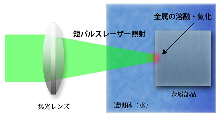
Non-thermal laser processing
Various processing system developments

Nano-Periodic Structure
Laser Peening Technology
deep compressive residual stress
Shared Technologies
Laser Processing Technology
- meri-second ~ femutosecond laser processing
- CW(Continuous wave) laser Processing
optical measurement of Laser Processing
- Ultrafast Phenomena Measurement (high-speed camera, high-speed streak camera)
- spectroscopy[Plasma emission, Raman scattered light]
- Weak light measurement[PMT, Cooled CCD, fluorescent plate ]
device development
- machining head, Machining system design
- Medical device development
- Measurement of Laser processing, Optical system design
- ※Participation in projects(Base generation project to create a next-generation light and healthcare industry in Hamamatsu)
human resources development
- Training of laser processing specialists